基站

用于无线基础设施的高效电源方案
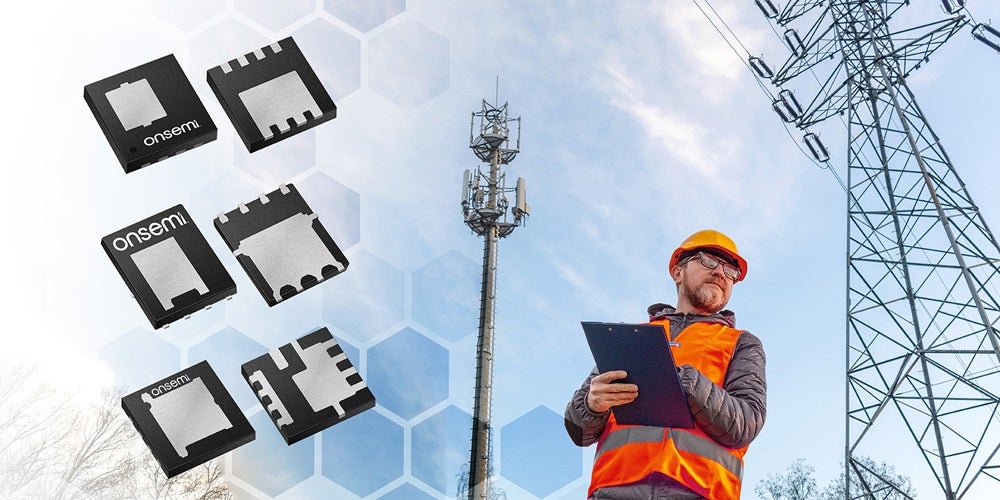
基站是5G乃至未来6G无线网络的基础,为移动宽带、工业物联网、私有网络以及AI应用提供高速连接、低时延和可靠的通信。 随着网络流量持续增长,运营商正部署宏基站、大规模MIMO系统和小单元基站,以提升容量、扩大覆盖范围并提高频谱效率。
现代基站依赖于高效能48V电源架构和先进的电源转换技术,以满足日益增长的性能和能效需求。 宽禁带半导体(包括碳化硅MOSFET、碳化硅级联JFET和氮化镓功率器件)可实现更高的功率密度、更低的损耗、更优的散热性能以及更低的运营成本。这些技术支持下一代电源、射频系统和分布式网络部署。
典型的基站集成了AC-DC电源、基带单元(BBU)、远程射频单元(RRU)、有源天线单元(AAU)、射频前端、时序电路以及PoL供电解决方案。 随着网络向开放式无线接入网(Open RAN)和基于云的架构演进,用于高效供电、精密传感、保护和同步的半导体解决方案正变得至关重要,以确保电信基础设施具备可扩展性、可靠性和面向未来的能力。


Previous
Next
产品
Low/Medium Voltage MOSFETs
Portfolio of comprehensive range of Low-medium voltage power Mosfets that delivers superior performance and reliability for switching applications. Our cutting-edge PowerTrench® T10 technology delivers industry leading RDS, higher power density, reduced switching losses and better thermal performance.
Silicon Carbide (SiC) MOSFETs
Our SiC MOSFETs are designed to be fast and rugged and include system benefits from high efficiency to reduced system size and cost. MOSFETs are metal–oxide–semiconductor field-effect transistors with insulated gates. These silicon carbide MOSFETs have a higher blocking voltage and higher thermal conductivity than silicon MOSFETs, despite having similar design elements. SiC power devices also have a lower state resistance and 10 times the breakdown strength of regular silicon. In general, Systems with SiC MOSFETs have better performance and increased efficiency when compared to MOSFETs made with silicon material.
There are many advantages to choosing SiC MOSFETs over silicon MOSFETs, such as higher switching frequencies. High-temperature development is also not a concern when using SiC MOSFET modules because these devices can operate efficiently even in high heat. Additionally, with SiC MOSFETs, you benefit from a more compact product size because all components (inductors, filters, etc.) are smaller.
Silicon Carbide (SiC) Cascode JFETs
Our high-performance SiC Cascode JFETs utilize a unique cascode configuration, integrating a high-performance SiC fast JFET with a cascode-optimized Si-MOSFET.
Gallium Nitride (GaN) FETs
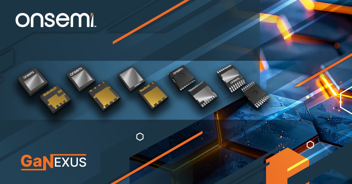
GaNEXUSTM Gallium Nitride (GaN) FETs are enhancement‑mode discrete GaN HEMTs that leverage wide‑bandgap material properties to deliver fast switching, low gate and output charge, and superior efficiency compared to silicon power transistors. These characteristics enable higher operating frequencies, reduced magnetics, and increased power density across low/medium, high and ultra-high voltage power conversion applications.
Gallium Nitride (GaN) Integrated Power
GaNEXUSTM Integrated Power includes GaNEXUS Drive, GaNEXUS Smart, and GaNEXUS Control, where each combines a GaN switch together with potential combination of additional features: gate driver, current sensing, protection, and control, in a single device to simplify design, reduce parasitics, and accelerate time to market.
AC-DC Power Conversion
Offline AC-DC controllers and regulators, and power factor and secondary side controllers that enable high active mode efficiency, low standby mode consumption and power factor correction.
Controllers
NCP81233
Multi-Phase Controller, Configurable, 4.5 V to 20 V, I2C
DC-DC Power Conversion
A product portfolio for DC-DC charge pumps, controllers, converters, and regulators.
Integrated Driver & MOSFET
Devices that combine driver IC with power MOSFETs and are optimized for DC-DC buck power conversion applications.
Current Sense Amplifiers
Current sensing requires accurate measurements and onsemi’s current sense amplifiers offer high degree of precision current sensing along with the advantages of wide input common mode range, bidirectional current sensing and high/low side current sensing.
LDO & Voltage Regulators
A portfolio that provides optimum solution for low power, space conscious and low noise designs.
Documents
White Papers
AI 数据中心和电信应用的电源技术对比
Tutorial
GaN Power Architectures Guide
Application Notes
Inside Elite Pairing Studio
Application Notes
Using Cascode SiC JFETs in LLC Primary
Collateral Brochure
工业级 LDO 选型指南
White Papers
High Performance, Precision Analog Capability Enabled by the Treo Platform
Application Notes
How to Achieve 99.3% Efficiency in 3.6 kW Totem-pole PFC Using 750 V Gen 4 SiC Cascode JFETs
White Papers
onsemi EliteSiC M3S Technology for High-Speed Switching Applications
评估板/套件
Evaluation Board
NCP1681CCM1KWGEVB
CCM Totem pole PFC 1000 W design with Gate driver integrated GaNFETs
Evaluation Board
EVBUM2901G-EVB
Evaluation Board for Double Pulse Testing discrete solutions
Evaluation Kit
NCP81295GEVB
NCP81295GEVB Hot Swap Smart Fuse Evaluation Board
Evaluation Board
NCP3286GEVB
Evaluation board to support NCP3286. 40A Stackable Fixed Frequency Buck Regulator. DGSCOMEVB USB dongle for PMBUS functionality sold separately


常见问题解答
氮化镓技术可实现高频开关、紧凑型电源转换以及效率提升。通过缩小磁性元件尺寸和系统占用空间,氮化镓技术支持更高的功率密度并简化了集成。它非常适合用于DC-DC转换、高密度电源以及下一代电信平台——在这些应用中,热管理、可扩展性和缩小系统尺寸是关键的设计目标。
碳化硅器件在降低开关损耗和导通损耗的同时,还能支持更高的开关频率并提升散热性能。它们在高压交流-直流转换、功率因数校正(PFC)以及中间母线级中表现尤为出色。这些特性有助于工程师在多千瓦级电信电源系统中实现更高的功率密度、更高的能效、更低的散热要求以及更高的可靠性。
未来基站的设计正受到人工智能应用、大规模物联网部署、云服务、工业自动化以及日益增长的移动数据流量的推动。 这些趋势正在加速大规模MIMO、高功率无线电架构、宽禁带(WBG)半导体、高效率电源、先进热管理以及可扩展供电系统的采用,这些技术既支持5G,也支持未来的6G基础设施。
大规模MIMO系统通过大型天线阵列和波束成形技术来提升网络容量,但同时也显著增加了功耗、热密度和同步要求。工程师必须在优化射频功率传输、热管理、时序精度和电源转换效率的同时,确保系统在户外部署环境中,通过众多收发信道保持可靠运行。
波束成形、载波聚合、协调多点传输以及时分双工(TDD)等先进的5G功能,需要基带系统与无线系统之间实现高度精确的同步。 IEEE 1588v2精密时间协议(PTP)和SyncE等技术有助于实现亚微秒级的时间对齐,从而提高网络可靠性、频谱效率和移动性性能,并支持新兴的私有无线和工业应用。
精选文章
为您精选的新闻和博文,挖掘创新灵感,洞见行业趋势。



精选视频
浏览相关视频,以全新视角,探索更多细节。


base stations